交流或电源适配器(或称适配器),也称为充电器,在便携式电子设备中将来自墙壁插座的交流电(AC)转换为直流电(DC)。由于适配器是无处不在的设备,有助于不断塞满任何旅行者的行李箱,它们应该尽可能地小和轻。如何利用现有技术实现这一目标?
AC or power adapters (or adapters), also known as chargers, convert alternating current (AC) from a wall outlet into direct current (DC) in portable electronic devices. Since adapters are ubiquitous devices that help constantly fill any traveler's suitcase, they should be as small and light as possible. How can this be achieved with existing technology?
最近在发表的论文亚洲及太平洋地区经济合作组织由罗姆和索霍大学的合著者一,说明了一种实现适配器小型化的新方法,使用开始开关以及初级侧的电压箝位和150V供电的不对称半桥(AHB)反激式转换器,以1MHz开关频率运行。
A recently published paper in APEC by Rohm and Soho University co-authors illustrates a new approach to adapter miniaturization, using a start switch as well as a voltage clamp on the primary side and a 150V powered asymmetrical half-bridge (AHB) flyback converter operating at a 1MHz switching frequency.
缩小适配器的困难
Narrowing adapter difficulties
在不损害安全性、效率或可靠性的情况下获得更小的尺寸始终是一项艰巨的任务。以适配器小型化为目标主要有两个障碍。第一个问题涉及输入电容小型化,但没有取得进展,因为较高的开关频率在这种情况下没有帮助。
Getting smaller sizes without compromising safety, efficiency or reliability is always a difficult task. There are two main obstacles to targeting adapter miniaturization. The first problem involved input capacitor miniaturization, but no progress was made because higher switching frequencies did not help in this case.
其次,对于平面变压器来说,减小变压器尺寸仍然是一个挑战,因为较少的匝数会导致较大的铁芯损耗。作者提出的拓扑结构允许输入电容和AHB变压器的尺寸减少大约50%。包括初级交流电压箝位器和AHB转换器的完整电路以90至264VAC输入电压和20V/3A输出实现。
Secondly, for planar transformers, reducing the transformer size is still a challenge, because fewer turns lead to larger core losses. The topology proposed by the authors allows the size of the input capacitance and AHB transformer to be reduced by approximately 50%. The complete circuit including the primary AC voltage clamp and AHB converter is implemented at 90 to 264VAC input voltages and 20V/3A outputs.
反激拓扑
Flyback topology
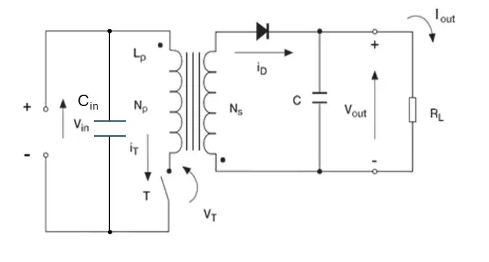
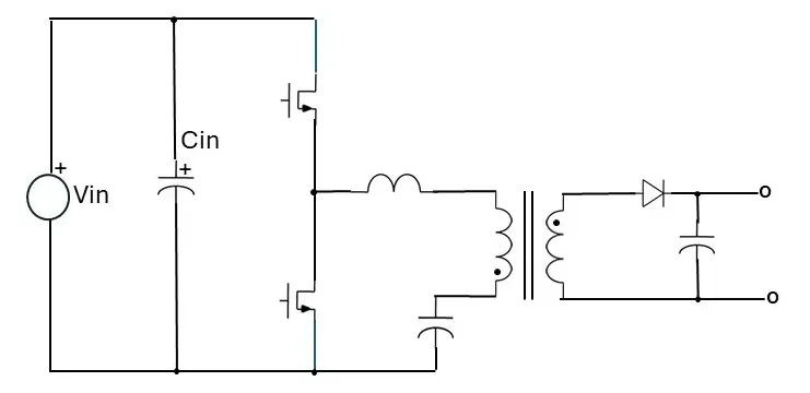
图1显示了一般的反激式拓扑结构,其工作原理是在开关周期的一半时间内将能量存储在磁场中,然后在另一半时间内将能量传递给负载。图2描述了AHB电路的实现。反激式转换器可以受益于GaN开关,在低频(比如100kHz)实现小型化,因为其固有的低导通电阻可以降低损耗。
Figure 1 shows the general flyback topology, which works by storing energy in the magnetic field for half of the switching cycle and then transferring it to the load for the other half. Figure 2 depicts the implementation of the AHB circuit. Flyback converters can benefit from GaN switches for miniaturization at low frequencies (such as 100kHz) because their inherent low on-resistance reduces losses.
相反,由于GaN FETs的存在,AHB可以在非常高的频率下工作,因此变压器可以在1MHz左右的频率下做得更小,从而实现更小的尺寸。“不对称”这一名称指的是两个开关在电压处理和驱动要求方面的不平衡,因为高端开关需要浮栅驱动,并且与低端开关相比,其电压应力更高。
In contrast, AHBs can operate at very high frequencies due to the presence of GaN FETs, so the transformer can be made smaller at frequencies around 1MHz, thus achieving a smaller size. The name "asymmetry" refers to the imbalance between the two switches in terms of voltage handling and drive requirements, as high-end switches require floating gate drive and have higher voltage stress compared to low-end switches.

图1:一般反激式转换器原理图
Figure 1: Schematic diagram of a general flyback converter
尽管这两种拓扑结构都实现了一定程度的小型化,但仍然存在一些问题,首先是输入电容Cin的大小。
Although both topologies achieve a degree of miniaturization, there are still some problems, starting with the size of the input capacitor Cin.

图2:不对称半桥反激式
Figure 2: Asymmetric half-bridge flyback
输入电容Cin由其在最低Vin时的储能能力决定,其耐受电压与最大Vin相关。换句话说,更高的开关频率无助于实现小型化。这同样适用于应承受400V电压的变压器,但平面结构中的匝数有限,因此提高频率是无效的,并会导致较大的铁芯损耗。平均而言,在典型的交流适配器中,Cin约占总体积的40%,变压器约占总体积的45%。
The input capacitor Cin is determined by its storage capacity at the lowest Vin, and its withstand voltage is related to the maximum Vin. In other words, higher switching frequencies don't help with miniaturization. The same applies to transformers that should withstand 400V voltage, but the number of turns in the planar structure is limited, so increasing the frequency is ineffective and will lead to large core losses. On average, in a typical AC adapter, Cin accounts for about 40% of the total volume, and the transformer accounts for about 45% of the total volume.
初级电压箝位器
Primary voltage clamp
为了克服这个缺点,可以提出一种结合初级电压箝位器和150V馈电AHB转换器的电路拓扑,这可以减小输入电容器和变压器的尺寸。借助150V GaN开关以1MHz的频率切换AHB转换器,可以缩小变压器。
To overcome this shortcoming, a circuit topology combining a primary voltage clamp and a 150V fed AHB converter can be proposed, which can reduce the size of the input capacitors and transformers. With the help of a 150V GaN switch to switch the AHB converter at a frequency of 1MHz, the transformer can be shrunk.

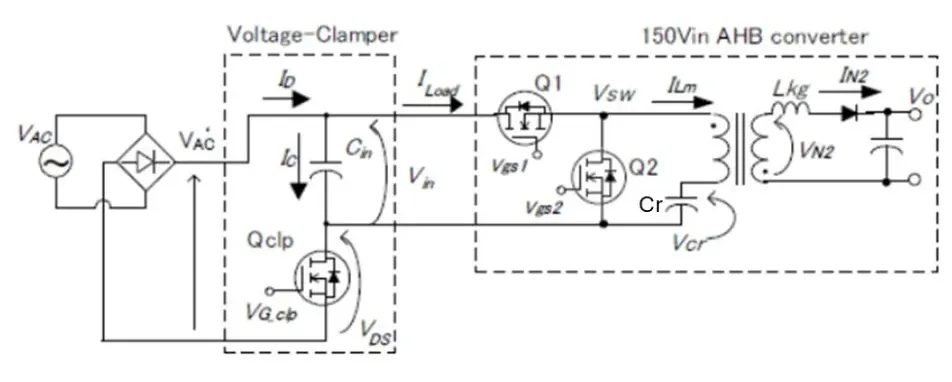
图3:建议的电路实现
Figure 3: Proposed circuit implementation
电压箝位器设计背后的思想与电容器中存储的能量有关,等于CV2因此,理论上,将其两端的电压减半将使大容量电容器的体积减小。一般来说,箝位器的功能是通过修改电压波形的DC电平来上移或下移电压波形。
The idea behind the design of a voltage clamp has to do with the energy stored in the capacitor, equal to CV2, so in theory, halving the voltage at its ends will reduce the volume of a high-capacity capacitor. In general, the function of the clamp is to shift the voltage waveform up or down by modifying the DC level of the voltage waveform.
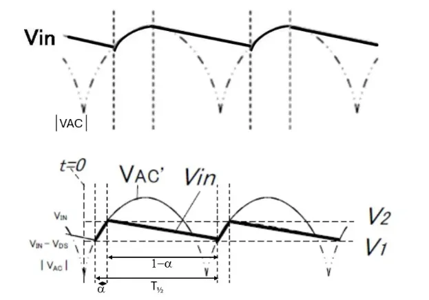
电路实现如图3所示,其中Qclp是箝位FET,输入电容Cin用于电压箝位。在最小输入电压(约100VAC)下,Qclp完全开启,以传统电容输入模式工作(图4a)。
The circuit implementation is shown in Figure 3, where Qclp is the clamping FET and the input capacitor Cin is used for voltage clamping. At the minimum input voltage (about 100VAC), the Qclp is fully turned on and operates in traditional capacitive input mode (Figure 4a).
在较高的输入电压下,电压箝位器被激活,如图4b所示。“VAC”是整流后的交流电压,Ic是通过Cin的充电电流。当VAC’到达V1时,Ic开始流动以对对应于角度α的Cin充电;所以,如果T是半周期,乘积在表示工作时间。当VAC到达V2时,Qclp关闭,这发生在Cin放电的角度(1-a)期间。
At a higher input voltage, the voltage clamp is activated, as shown in Figure 4b. "VAC" is the AC voltage after rectification, and Ic is the charging current through Cin. When VAC 'reaches V1, Ic begins to flow to charge Cin corresponding to Angle α; So, if T is half period, the product is representing the working time. Qclp turns off when VAC reaches V2, which occurs during Cin discharge at an Angle (1-a).

图4:不同时标下的主要波形:a)
低输入电压和b)高输入电压
Figure 4: Main waveforms at different time scales :a)
Low input voltage and b) High input voltage
150伏供电的AHB
150 volt powered AHB
半桥由Q1和Rohm的零件号GNE1040TB)驱动,开关节点连接到匝数比n = N1∶N2的变压器和谐振电容器Cr。图中的变压器是理想的,因此磁化电感Lm应与N1并联。漏电感Lkg串联连接到图中的N2。在次级侧,由于极性相反,二极管在关断时间内导通,允许功率传输。
The half-bridge is driven by the part number GNE1040TB of Q1 and Rohm, and the switching nodes are connected to the transformer and the resonant capacitor Cr with the turn ratio n = N1∶N2. The transformer in the figure is ideal, so the magnetizing inductor Lm should be in parallel with N1. The drain inductance Lkg is connected in series to N2 in the figure. On the secondary side, due to the opposite polarity, the diode is switched on during the off time, allowing power transfer.
AHB转换器可以在“电流谐振模式”和“连续电流模式”下工作。第二种操作看起来更有利,因为a)对于宽范围的输出电压的良好PWM控制,以及b)通过轻负载时磁化电流和重负载时漏电感电流的零电压开关(ZVS)能力。
The AHB converter can operate in both "current resonance mode" and "continuous current mode". The second operation looks more advantageous because of a) good PWM control for a wide range of output voltages, and b) Zero voltage switching (ZVS) capability to magnetize current through light loads and drain inductance current through heavy loads.
从CoilCraft中选择的平面变压器通常具有有限的匝数。计算条件为原边12匝,δB为70 mT,开关频率为1 MHz,标准交流输入的AHB输入总线电压为400 V,电压箝位为150 V。因此,400Vbus需要PL300内核,而150Vbus需要PL160内核,比PL300小2.7倍。通用设计方程如下所示。
Planar transformers selected from CoilCraft typically have a limited number of turns. The calculation conditions are 12 turns on the primary side, 70 mT δB, 1 MHz switching frequency, 400 V input bus voltage and 150 V voltage clamp for standard AC input AHB. Therefore, the 400Vbus requires a PL300 kernel, while the 150Vbus requires a PL160 kernel, which is 2.7 times smaller than the PL300. The general design equation is shown below.

其中DB是峰峰值磁场流量摇摆,V0是输出电压,D是占空比,T盐水是开关周期,Ae是有效核心的横截面积,NP是初级匝数。第二个是斯坦梅茨的经验公式,主要用于正弦激励:
Where DB is the peak-to-peak magnetic field flow swing, V0 is the output voltage, D is the duty cycle, T salt is the switching period, Ae is the cross-section area of the effective core, and NP is the number of primary turns. The second is Steinmetz's empirical formula, which is mainly used for sinusoidal excitation:

𝑃在哪里a𝑣是单位体积的时间平均功率损耗,单位为毫瓦每立方厘米,𝑓是频率在千赫,k,a,b是材料相关系数。高频下的铁芯损耗几乎完全是由涡流引起的,并且是大多数SMPS应用中最重要的铁芯限制。因此,作为一种折衷,磁通密度摆幅DB必须限制在比B小得多(美国)学业能力倾向测验(Scholastic Aptitude Test)从B-H滞后曲线来看。
𝑃 where a𝑣 is the time average power loss per unit volume in milliwatts per cubic centimeter, 𝑓 is the frequency in kilohertz, and k, a, and b are the material correlation coefficients. Core losses at high frequencies are almost entirely caused by eddy currents and are the most important core limitation in most SMPS applications. Therefore, as a compromise, the flux density swing DB must be limited to much smaller than B (US) as measured by the B-H lag curve on Scholastic Aptitude Test.
这篇文章中提到的论文旨在通过采用将初级电压箝位器与AHB转换器相结合的混合电路拓扑来减小交流适配器的尺寸。由于150V GaN FET开关工作在1MHz,将输入电容电压箝位至150 VDC可将输入电容的尺寸缩小50 %, AHB平面变压器也可缩小相同的尺寸。
The paper mentioned in this article aims to reduce the size of the AC adapter by adopting a hybrid circuit topology that combines a primary voltage clamp with an AHB converter. Since the 150V GaN FET switch operates at 1MHz, clamping the input capacitor voltage to 150 VDC reduces the size of the input capacitor by 50%, and the AHB flat transformer reduces the size by the same amount.